 EN
EN

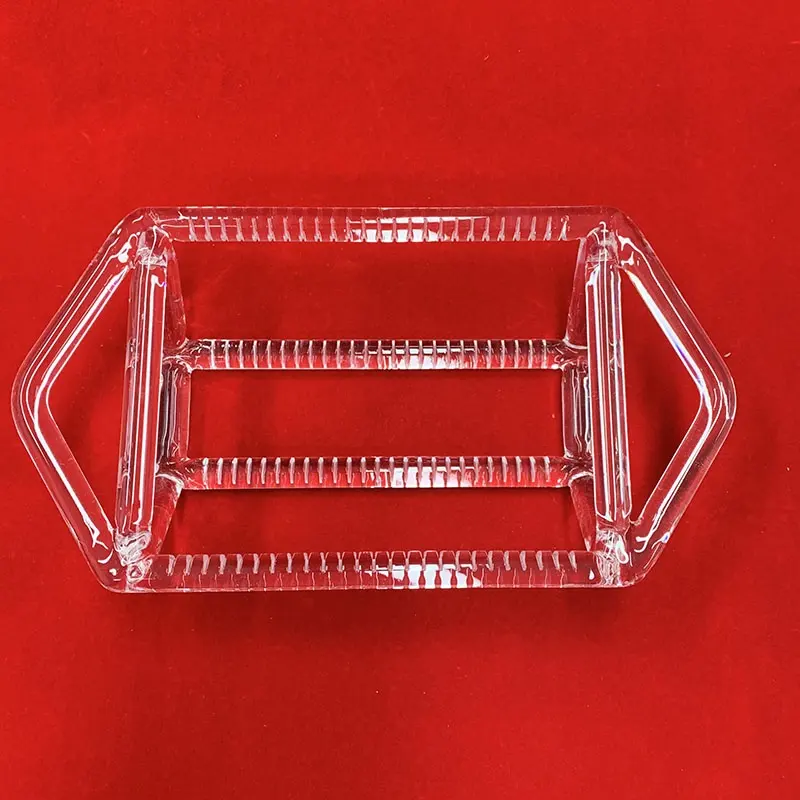
The Critical Foundation of Silicon Substrates and Optical Carriers
Modern microelectronics and semiconductor device fabrication operate under microscopic tolerances where absolute material perfection directly dictates yield rates. Within cleanroom environments, process engineers rely on specialized carrier substrates and optical windows to support delicate photolithography, wafer handling, and deposition workflows. Standard glass or low-grade ceramic materials frequently fail under the rigorous chemical and physical demands of modern cleanroom protocols, leading to contamination or structural failure. Senior semiconductor packaging specialists and process metallurgists consistently observe that selecting premium substrate materials prevents costly batch rejections and ensures consistent device performance. Navigating these demanding environments requires an engineered material that combines extreme purity with mechanical resilience. A quartz wafer serves as an indispensable asset in these advanced production lines, providing a robust, ultra-clean platform designed to withstand the punishing realities of microfabrication.
Thermal Stability and Dimensional Accuracy Across High-Temperature Steps
Semiconductor manufacturing routinely involves exposing components to extreme thermal processing, including high-temperature oxidation, annealing, and chemical vapor deposition. During these intensive heating cycles, materials are prone to thermal expansion, micro-warping, and dimensional distortion that can ruin fine circuit geometries. Conventional substrates often expand unevenly, introducing mechanical stress that compromises alignment accuracy. Fused silica features an extraordinarily low coefficient of thermal expansion, ensuring that the atomic matrix remains dimensionally stable even when subjected to rapid thermal ramps exceeding one thousand degrees Celsius. Process engineers rely on this exceptional thermal resilience to maintain strict lithographic tolerances and prevent carrier deformation, ensuring that every batch maintains exact geometric precision throughout complex manufacturing sequences.
Unmatched Chemical Resistance in Wet Etching and Cleaning Cycles
Fabrication workflows require frequent exposure to aggressive chemical reagents, including concentrated hydrofluoric acid baths, strong alkaline solutions, and reactive ion etching plasmas designed to strip organic residues or etch microscopic patterns. Many standard structural materials degrade rapidly under these harsh conditions, releasing particulate contaminants that ruin sensitive semiconductor layers. High-purity quartz exhibits phenomenal resistance to almost all chemical agents, maintaining a completely stable surface that resists pitting and chemical leaching. Field experience from wet-bench supervisors confirms that utilizing chemically inert substrates drastically reduces particle generation during rigorous cleaning cycles, protecting valuable microelectronic components from destructive contamination and extending the operational lifespan of production hardware.
Optical Clarity and Transmission Performance for Photolithography
Beyond mechanical and chemical robustness, advanced microfabrication frequently demands superior optical transmission capabilities, particularly across ultraviolet and deep ultraviolet spectrums. During mask alignment, laser inspection, and optical metrology procedures, any attenuation or scattering of light waves can introduce critical alignment errors. Fused silica features exceptional optical clarity and a high transmittance rate across a broad wavelength range, allowing light beams to pass through the substrate with minimal energy loss. Quality control technicians and optical engineers utilize these pristine substrates to ensure flawless inspection results and precise laser patterning, eliminating optical distortion and ensuring that micro-scale features are reproduced with absolute fidelity.
Translating Material Superiority Into Lasting Manufacturing Success
Selecting the correct foundational substrate directly influences the overall productivity, yield reliability, and economic viability of modern semiconductor production. By completely eliminating thermal distortion, chemical degradation, and optical interference, fabrication facilities drastically reduce manufacturing defects and prevent catastrophic batch losses. Reliable substrate materials transform unpredictable processing steps into highly standardized, repeatable industrial operations. Highborn leverages advanced fabrication expertise and stringent cleanroom quality control protocols to produce exceptional quartz components designed for demanding electronics environments. Through a robust, globally integrated supply chain, Highborn ensures that semiconductor manufacturers and research laboratories have continuous access to the precision hardware necessary to keep production lines running smoothly. Dedicated material engineering transforms raw high-purity silica into a strategic operational advantage, empowering global tech industries to scale advanced device fabrication with absolute confidence.
Table of Contents
- The Critical Foundation of Silicon Substrates and Optical Carriers
- Thermal Stability and Dimensional Accuracy Across High-Temperature Steps
- Unmatched Chemical Resistance in Wet Etching and Cleaning Cycles
- Optical Clarity and Transmission Performance for Photolithography
- Translating Material Superiority Into Lasting Manufacturing Success

