I. Performance Foundation: The Comprehensive Advantages of SiC
The core structural components employed in semiconductor manufacturing equipment are routinely subjected to simultaneous exposure to severe thermal cycling and substantial mechanical loading, a dual-demand scenario that imposes a multiplicity of stringent performance constraints on any candidate material system. Among the various engineering material families that are currently available for such demanding applications, precision ceramics have increasingly emerged as a preferred solution for high-end semiconductor equipment parts, owing to their unique and often unparalleled combination of physical, mechanical, and chemical attributes. Within this broader category of advanced ceramics, silicon carbide (SiC) stands out as a particularly representative structural ceramic, distinguished by an exceptional suite of properties: outstanding flexural strength, remarkable hardness, and a high elastic modulus, coupled with superior specific stiffness and thermal conductivity, a notably low coefficient of thermal expansion, and extraordinary resistance to chemical corrosion in aggressive environments. As a result of this favorable property portfolio, SiC has already achieved widespread and mature industrial adoption across a diverse range of sectors, including petrochemical processing, general mechanical engineering, nuclear reactor technology, and microelectronics fabrication, thereby attesting to its versatility and reliability under varied operational conditions.
II. Machining Adaptability and Structural Design Potential
Beyond its intrinsically superior fundamental physicochemical characteristics, silicon carbide also exhibits favorable machinability, particularly with respect to polishing processes, which renders it highly suitable for the production of functional components demanding exceptionally smooth surface finishes, such as precision reflectors and vacuum chucks used in lithographic systems. Through carefully controlled grinding and polishing sequences, SiC workpieces can be brought to a mirror-like surface quality, and once such a high-grade surface finish is achieved, the resulting components demonstrate minimal susceptibility to thermally induced distortion or mechanically driven deformation, even when subjected to fluctuating operational environments. In parallel with this surface-processing advantage, the material's mechanical robustness allows for the implementation of innovative lightweight topological designs, wherein strategic material removal or structural optimization is employed to achieve significant mass reduction without compromising stiffness or dimensional stability. This capability is particularly beneficial for the fabrication of guide rails, stage assemblies, and other moving or load-bearing parts, where reduced inertia and enhanced dynamic response are critical, thereby making SiC an eminently suitable choice for meeting the practical demands of modern high-end semiconductor equipment, which increasingly emphasizes both weight minimization and long-term form stability.
III. Practical Challenges in Fabrication Processes
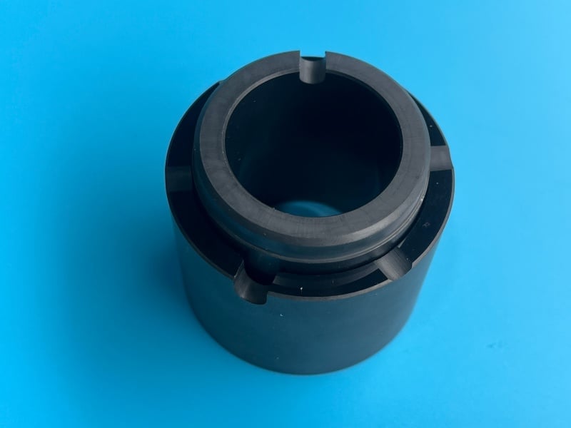
Notwithstanding the numerous and substantial advantages that silicon carbide offers, it must be acknowledged that the material belongs to a strong covalent bonding system, a fundamental characteristic that inherently confers high hardness and pronounced brittleness. These very attributes, while beneficial for wear resistance and dimensional retention, simultaneously impose considerable technical difficulties when it comes to the precision machining of SiC-based ceramic plates, rings, rods, and other geometrically intricate parts, often necessitating the use of diamond tooling and specialized processing strategies to avoid surface damage or edge chipping. Moreover, achieving full densification in SiC ceramics requires exposure to exceedingly high sintering temperatures, typically well in excess of 2000°C, and obtaining a final product that simultaneously exhibits high density and dimensional proximity to the net shape demands a thoroughly developed and rigorously controlled sintering protocol, encompassing factors such as heating rate, dwell time, atmosphere composition, and pressure application. The fabrication challenges become even more formidable when dealing with large-scale components, hollow thin-walled structures, or complex, non-axisymmetric cavity-type custom parts, all of which require a high level of process integration, including near-net-shape forming, controlled shrinkage management, and post-sintering finishing. The sustained commitment to overcoming these fabrication hurdles is not an academic exercise but a practical necessity, driven by the uncompromisingly severe performance criteria that semiconductor equipment imposes on every constituent part, where even minor defects or dimensional deviations can lead to catastrophic failure or yield loss.
IV. Comprehensive Performance Thresholds for Semiconductor Equipment
Semiconductor manufacturing equipment, during its normal operational cycles, is subject to a demanding array of environmental and mechanical stresses, including rapid temperature variations, high-vacuum conditions, and continuous precision mechanical movements, all of which collectively establish multiple hard constraints on the mechanical strength, thermal behavior, and environmental resilience of the accompanying components. To illustrate this point, one may consider the lithography machine, which stands as the cornerstone of front-end semiconductor processing and integrates advanced technologies spanning optics, materials science, precision control, and computational algorithms; the internal parts of such a machine cannot be evaluated on the basis of any single property in isolation, but must simultaneously attain elevated performance levels across a broad spectrum of criteria. For key functional components intended for deployment in semiconductor equipment, the base material must therefore satisfy a well-defined set of comprehensive threshold requirements: ultra-high purity to prevent metallic contamination, near-theoretical density to eliminate porosity-related weaknesses, high flexural strength to withstand mechanical loads, a high elastic modulus to preserve positional accuracy under force, outstanding thermal conductivity to efficiently dissipate localized heat, and a low thermal expansion coefficient to minimize misalignment induced by temperature drift. Beyond these intrinsic material properties, the finished components themselves are further required to demonstrate extraordinarily tight geometric dimensional tolerances and the ability to realize complex, often asymmetric, three-dimensional configurations that are tailored to specific equipment layouts. Precision ceramic materials, and silicon carbide in particular, are uniquely positioned to satisfy this multifaceted and interlinked set of demands, thereby justifying their growing prominence in the semiconductor equipment supply chain.


 EN
EN