 EN


Why Thick Film Circuit Is Widely Adopted for Electronic Sensing Modules
Electronic sensing modules often have to do more than read a signal. They may sit near heat sources, switch loads, operate in compact housings, or carry a sensor output into conditioning and control circuitry. That mix explains why a thick film circuit is widely adopted in these designs. It gives engineers a practical way to place conductors, resistive elements, and insulating layers on one ceramic base while keeping the layout focused on the actual sensing task.
From an application-engineering viewpoint, the useful question is not whether thick-film technology is universally superior. It is whether the sensing module needs a stable substrate, integrated passive functions, a compact interconnect layout, or a process that can be adapted to the required geometry. When those conditions matter, a thick film circuit can be a strong fit.
What a Thick Film Circuit Adds to a Sensing Module
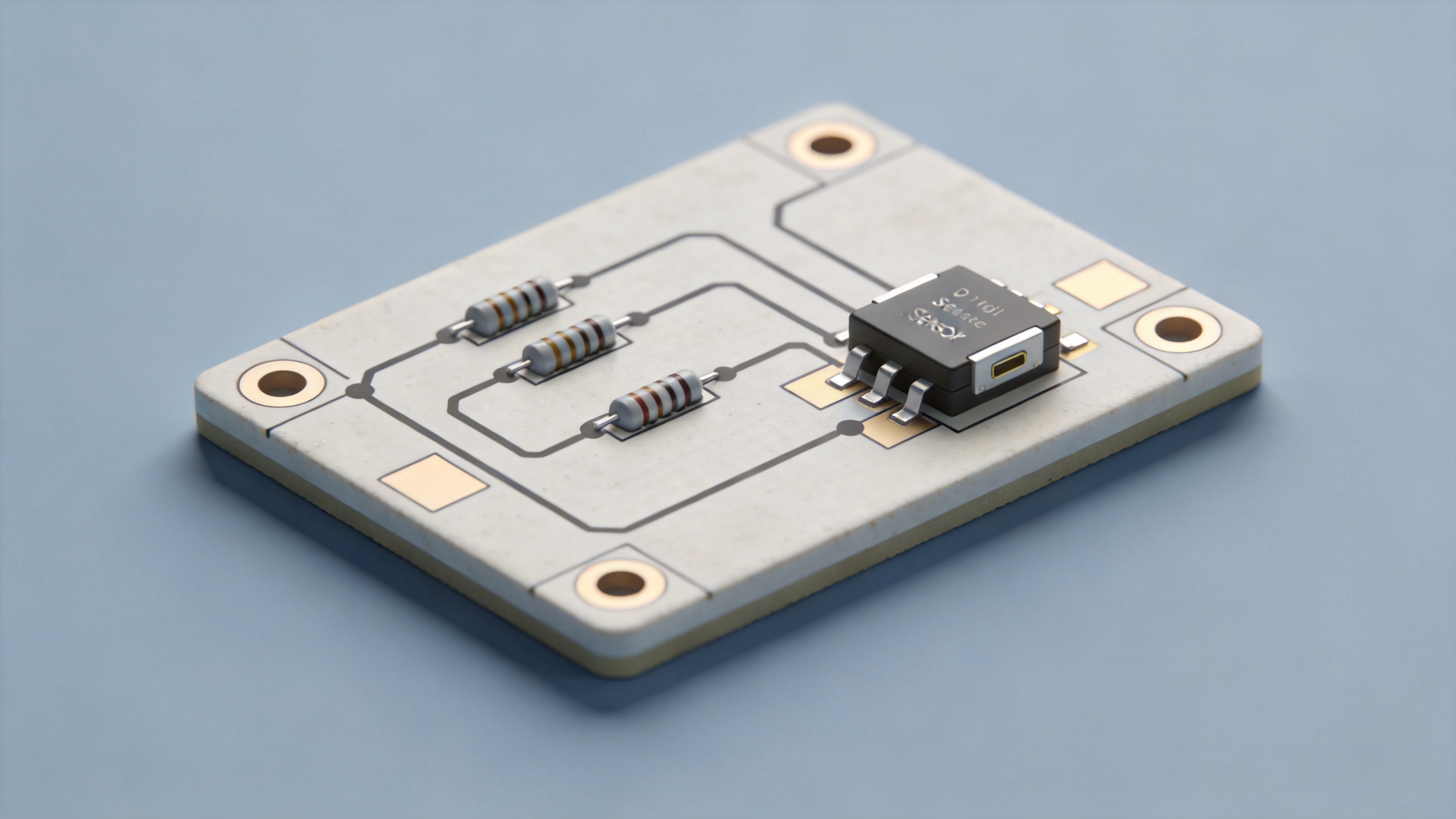
A thick film circuit is commonly made by screen-printing conductive, resistive, and dielectric pastes in patterned layers on a ceramic substrate. The printed layers are dried and fired so the functional materials bond to the substrate. This approach is different from simply mounting discrete parts on an organic board: parts of the interconnect and passive network can be formed directly on the base.
For a sensing module, that construction can bring the sensor connection boundary, signal-conditioning resistors, protective elements, and connection pads into a controlled physical stack. The resulting design still needs appropriate component selection and verification, but it can reduce unnecessary connection boundarys between the sensing element and the rest of the circuit.
Why Ceramic Substrates Matter in Sensor Electronics
The substrate is a major reason a thick film circuit is considered for demanding sensor electronics. A ceramic resistor network or conductor pattern is supported by a rigid, dimensionally stable base rather than a flexible organic laminate. In applications with heat, thermal cycling, or a small metal enclosure, that difference can affect layout decisions, attachment methods, and long-term signal stability.
Metallized ceramic is especially relevant when a module needs a robust connection boundary between circuit features and other mechanical or electrical elements. The metalized areas may provide attachment or connection surfaces, but the correct metallurgy, geometry, and joining process depend on the specific design. It is more accurate to treat metallized ceramic as a system-level connection boundary choice than as a standalone reliability claim.
Thermal behavior should also be viewed in context. Ceramic can help move or tolerate heat differently from an organic board, yet the outcome depends on substrate material, thickness, copper or printed conductor area, mounting, power dissipation, and enclosure design. A module that includes a high voltage resistor or a heat-generating element needs a complete thermal and clearance review, not an assumption based on substrate type alone.
Integrated Resistors Support Compact Signal Conditioning
Many sensing circuits require more than one passive value: a bias path, a divider, a gain-setting network, a pull-up or pull-down, or a protection path. With thick-film processing, a thick film resistor pattern can be printed as part of the circuit architecture. This can be useful where available area is limited or where a resistor network benefits from being close to the sensing path.
The value of that approach is not merely smaller packaging. Integrating passive patterns can simplify how a designer manages nodes, pads, and routing inside a module. It can also make trimming and tolerance planning part of the manufacturing discussion where the selected process supports it. Still, resistance tolerance, temperature coefficient, noise, stability, and voltage loading should be specified for the actual circuit. A thick film resistor is not interchangeable with every thin-film or discrete-resistor option.
High-Voltage and Isolation Requirements Need Layout Discipline
Some sensing modules monitor mains-related equipment, ignition systems, industrial power supplies, or other elevated-potential circuits. In those cases, a high voltage resistor may be part of a divider, a discharge path, or a protective network. Thick-film construction can support compact layouts, but compactness should not reduce the attention given to creepage, clearance, resistor voltage distribution, contamination exposure, and transient conditions.
A practical review sequence is to identify the working voltage and expected transient environment, define the required separation distances for the relevant application, then examine how the resistor network, printed conductor edges, terminals, and enclosure interact. If the circuit will be potted, exposed to moisture, or mounted on metal, those conditions belong in the review as well. This is where a ceramic resistor implementation may help the layout, but it does not replace electrical safety analysis.
Manufacturing Flexibility Matches Sensor-Module Geometry
Sensor packages frequently have irregular outlines, specific connector locations, mounting holes, or limited height. Screen-printed layers let a thick film circuit follow a purpose-built pattern on the selected substrate. That can be useful for hybrid assemblies where a sensing element, connector, and passive network must share a small footprint.
The manufacturing conversation should start early. Engineers and buyers can clarify substrate dimensions, active areas, conductor pattern, resistor locations, termination method, expected operating conditions, and acceptance criteria before treating the circuit as a standard board. For custom modules, a drawing and the intended test conditions are often more informative than a short material name.
Where Thick Film Is a Good Fit—and Where It May Not Be
Thick-film technology is often considered when a sensing module needs ceramic-based construction, integrated passive functions, environmental robustness, or a compact hybrid layout. Typical decision signals include a hot mounting location, a need to keep a resistor network close to the sensor, a mechanical need for metallized ceramic connection boundarys, or a high-voltage section that needs carefully planned spacing.
It may be less suitable when the primary goal is the lowest-cost, high-volume organic PCB, when exceptionally tight resistor precision is the only driver, or when the circuit’s high-frequency behavior requires another interconnect approach. More precisely, the decision should come after comparing electrical targets, environment, volume, geometry, manufacturing route, and validation plan.
A Practical Specification Checklist
- What does the sensor measure, and what signal-conditioning functions are required?
- What temperature range, cycling profile, vibration, humidity, or contamination conditions will the module experience?
- Which resistor values, tolerances, voltage stresses, and stability requirements apply to each network?
- Does the module require a high voltage resistor, and what creepage, clearance, and transient conditions must be addressed?
- Is metallized ceramic needed for attachment, terminals, shielding, or heat-transfer connection boundarys?
- What substrate geometry, connector location, mounting method, test method, and acceptance criteria should be shown on the drawing?
Conclusion
A thick film circuit is widely adopted for electronic sensing modules because it combines ceramic-based support with printed conductors, resistor patterns, and insulating layers in a compact, application-specific layout. Its real advantage is the ability to align circuit construction with sensor placement, thermal conditions, voltage requirements, and mechanical connection boundarys. Before finalizing a design, confirm the actual operating environment and the electrical, dimensional, and validation requirements. That turns a general materials choice into an engineering decision that can be tested.

