Quartz Wafers for Semiconductors: High-Purity, Customizable

Get a Free Quote

Our representative will contact you soon.
Email
Mobile/WhatsApp
Name
Company Name
Message
0/1000
Unmatched Quality and Versatility of Quartz Wafers

Unmatched Quality and Versatility of Quartz Wafers

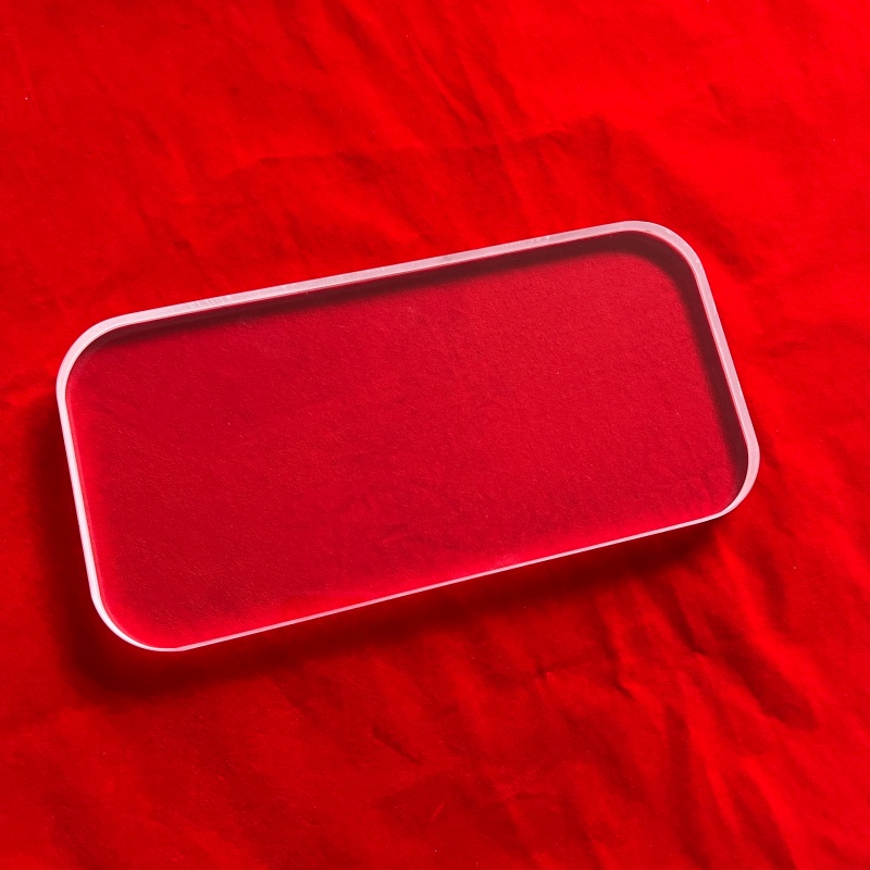
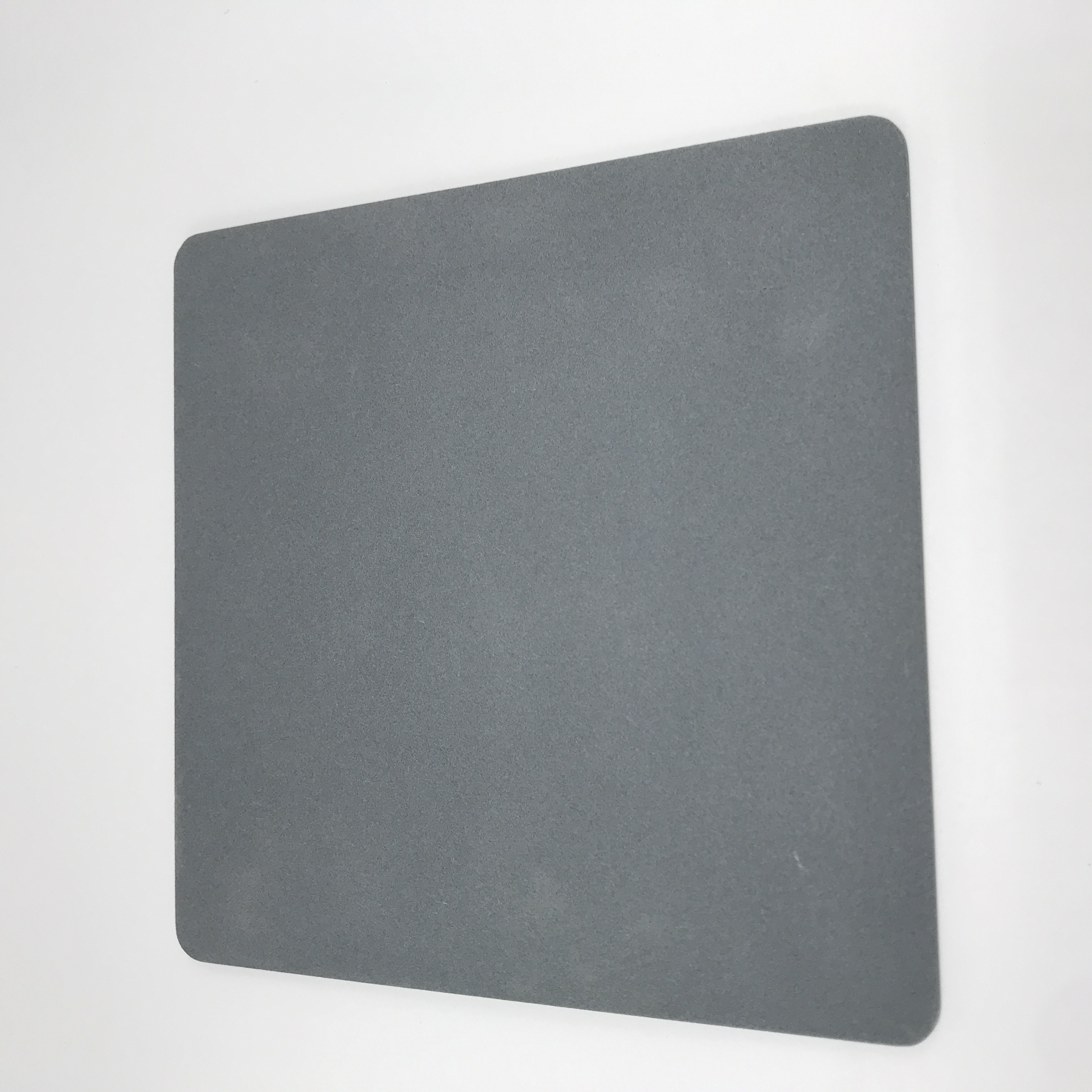
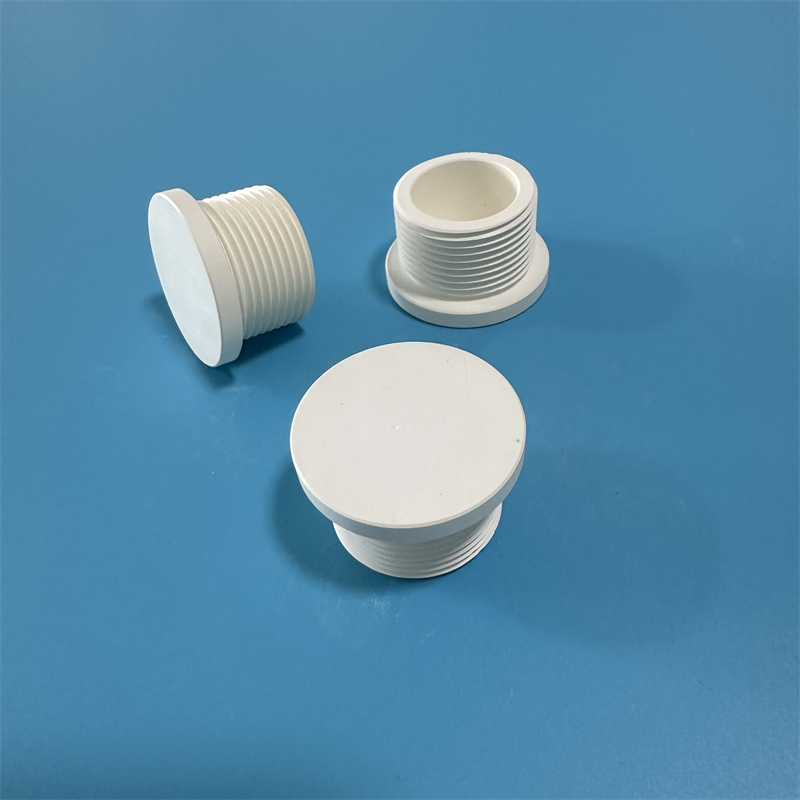
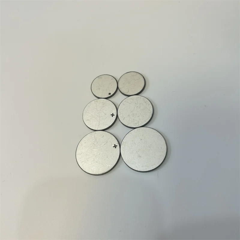
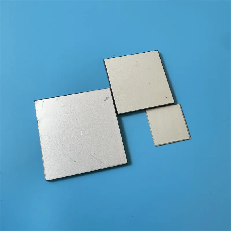
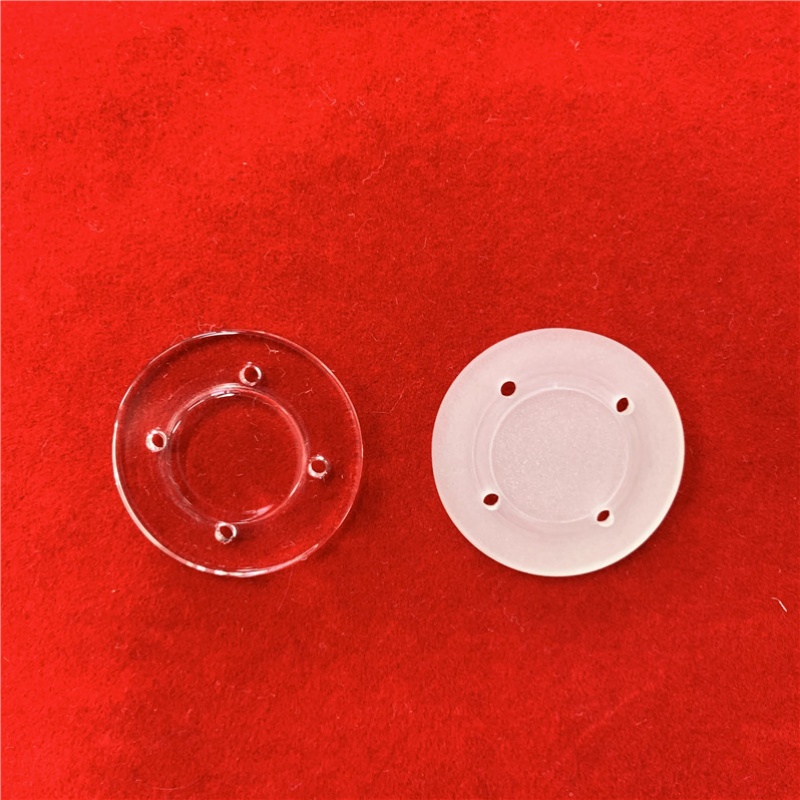
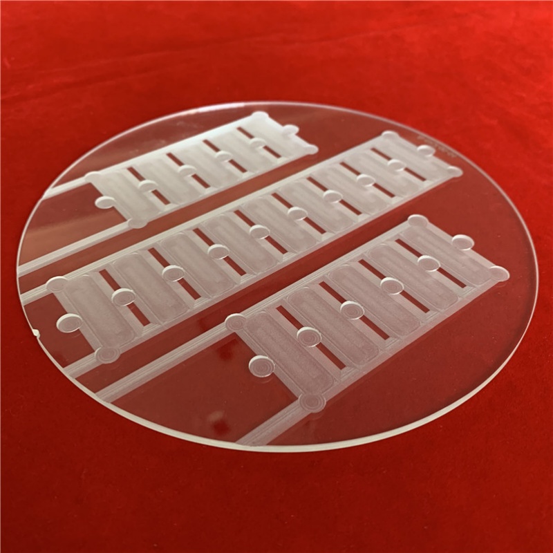
Quartz wafers are critical components in the semiconductor industry, renowned for their exceptional thermal and chemical stability. Highborn Group, with over 20 years of experience, leverages advanced technology to produce high-quality quartz wafers that cater to diverse applications, including electronics and optics. Our wafers are manufactured in five state-of-the-art facilities, ensuring consistency and reliability. With certifications such as ISO9001 and FDA, we guarantee that our products meet the highest quality standards. Our quartz wafers have been utilized in over 1,000 projects worldwide, demonstrating their effectiveness in enhancing device performance and longevity.
Get A Quote

Case Study

Enhancing Semiconductor Performance

A leading semiconductor manufacturer faced significant thermal management bottlenecks that hindered the performance and lifespan of their latest chip architectures. By integrating Highborn’s precision-engineered quartz wafers into their thermal management stack, they achieved a transformative 30% increase in device thermal conductivity. This innovation effectively dissipated heat, reducing energy consumption and drastically extending the operational lifespan of their electronic components. The resulting design efficiency led to verified annual cost savings exceeding $500,000. This case illustrates how high-purity quartz substrates act as a critical performance catalyst, allowing semiconductor leaders to push the boundaries of energy efficiency and hardware longevity in highly competitive global markets.

Optical Clarity in Precision Instruments

A renowned optics company required a substrate material that could provide superior transparency while maintaining extreme mechanical durability for their next-generation precision instruments. Standard glass options were prone to degradation and signal loss, which negatively impacted end-user satisfaction. After switching to Highborn’s high-purity quartz wafers, the company recorded a 25% increase in total light transmission efficiency, which directly resulted in a sharper, more reliable output for their optical systems. This performance jump was so significant that the company reported positive feedback from over 95% of their customers. This success highlights the indispensable role our quartz technology plays in elevating the standards of precision optical instrumentation.

Custom Solutions for Unique Applications

A fast-growing startup developing innovative sensor technology struggled to find a standard substrate that met their unique dimensional and structural requirements. Highborn Group collaborated directly with their engineering team to develop customized quartz wafers tailored precisely to their sensor specifications. This bespoke approach not only improved the accuracy of their final product but also streamlined their manufacturing process, reducing total production costs by 15%. The success of this collaboration allowed the startup to accelerate their product development cycle and successfully launch their sensors in multiple international markets. This project demonstrates our ability to translate unique technical requirements into optimized quartz solutions that drive business success.

Related products

Quartz wafers are integral to modern technology, particularly in the semiconductor and optics industries. The production process involves sourcing high-purity quartz, followed by meticulous fabrication techniques to achieve the desired thickness and surface quality. At Highborn Group, we employ advanced machinery and rigorous quality control measures to ensure that each wafer meets stringent specifications. Our commitment to research and development has led to over 40 patents, allowing us to innovate continuously and provide tailored solutions for our clients. With a global footprint across 126 countries, our quartz wafers have been proven in various applications, including solar cells, sensors, and precision optics. The versatility and reliability of our products make them the preferred choice for businesses looking to enhance their technological capabilities.

Frequently Asked Questions

What are quartz wafers used for?

Quartz wafers are primarily used in the semiconductor industry for manufacturing electronic components, as well as in optics for precision instruments. Their thermal stability and chemical resistance make them ideal for these applications.
We implement rigorous quality control processes, including ISO9001 certification, to ensure that every quartz wafer meets industry standards for purity and performance.
Yes, we offer customization options for quartz wafers to meet specific client requirements, including size, thickness, and surface finish.
Our company holds several certifications, including ROHS, CE, MSDS, ISO, SGS, TÜV, LVD, and FDA, ensuring compliance with international quality standards.

Related articles

How Does Boron Carbide Enhance Durability in Abrasive Blasting Nozzles?

17

Nov

How Does Boron Carbide Enhance Durability in Abrasive Blasting Nozzles?

Discover how boron carbide's extreme hardness and thermal stability deliver 5x longer lifespan than steel and 62% lower operating costs in abrasive blasting. See real field data and ROI insights.
View More
Piezo PZT Ceramic Ring: Enabling Precise Actuation in Medical and Industrial Devices

23

Oct

Piezo PZT Ceramic Ring: Enabling Precise Actuation in Medical and Industrial Devices

Discover how PZT ceramic rings enable sub-micron precision in surgical robots, fuel systems, and optical alignment. 30% more responsive than alternatives. Learn more.
View More
Piezoelectric Ceramics: Improving Sensor Performance in Medical Devices

17

Nov

Piezoelectric Ceramics: Improving Sensor Performance in Medical Devices

Discover how piezoelectric ceramics enhance medical sensor precision, improve ultrasound imaging by 40%, and enable minimally invasive surgery. Learn about real-world clinical benefits and adoption challenges. Explore the future of healthcare sensing technology.
View More
Why Is Boron Carbide Ceramic Used in Lightweight Armor Applications?

18

Nov

Why Is Boron Carbide Ceramic Used in Lightweight Armor Applications?

Discover why boron carbide ceramic dominates lightweight armor applications with 30-40% less weight, superior hardness, and proven ballistic performance. Learn how it enhances soldier mobility and mission success.
View More

Customer Testimonials

John Smith
Exceptional Performance and Support

Highborn's quartz wafers significantly improved our product performance. We saw a 20% increase in efficiency!

Sarah Johnson
Reliable and High-Quality Products

Their customized solutions helped us launch our product on time, with remarkable accuracy and durability. Highly recommended!

Get a Free Quote

Our representative will contact you soon.
Email
Mobile/WhatsApp
Name
Company Name
Message
0/1000
Unmatched Quality Assurance

Unmatched Quality Assurance

At Highborn Group, we operate under a philosophy that uncompromising quality is the baseline for success in the high-stakes semiconductor and optics industries. Every quartz wafer we produce undergoes a multi-stage, rigorous quality assurance protocol that screens for structural defects, surface impurities, and dimensional deviations. By maintaining ISO9001, FDA, and various international safety certifications, we provide a layer of institutional trust that allows our clients to integrate our components into their mission-critical hardware with total peace of mind. This relentless commitment to material purity and manufacturing consistency is what separates our wafers from standard industrial alternatives, ensuring that your devices operate at the highest possible performance tier and maintain their integrity over the long term, ultimately minimizing your technical risk in a demanding global market.
Innovative Customization Capabilities

Innovative Customization Capabilities

We recognize that modern technological innovation often requires bespoke physical and material architectures that cannot be satisfied by mass-market options. Highborn Group thrives on this complexity; our R&D team works in direct, collaborative partnership with your design engineers to develop quartz wafers that meet your specific thickness, diameter, surface finish, and doping requirements. By integrating our extensive intellectual property—backed by over 40 patents—into your design phase, we create high-performance substrates that significantly improve the operational efficacy of your sensors, solar cells, or optical components. This flexibility does not just solve a manufacturing challenge; it acts as a strategic upgrade to your product design, leading to measurable gains in accuracy, performance longevity, and overall client satisfaction that keep your business ahead of the curve.
email goToTop